
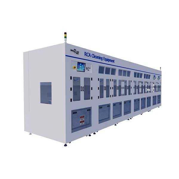
| 1. Overview of RCA cleaning machine
RCA cleaning is a wafer surface cleaning process widely used in the semiconductor, microelectronics, and photovoltaic industries, developed by RCA Corporation in the 1960s. RCA cleaning machine is an automated equipment specifically designed to perform this process, which removes organic matter, metal ions, and particulate pollutants from the wafer surface through chemical solutions and deionized water, ensuring high cleanliness during the chip manufacturing process. |
 |
2. Core cleaning process steps
RCA cleaning usually consists of the following two steps (the order or combination can be adjusted according to needs):
SC1 Cleaning (APM)
Solution: Ammonia (NH ₄ OH)+Hydrogen peroxide (H ₂ O ₂)+Deionized water (H ₂ O)
Function: Remove organic residues and particles, while slightly oxidizing the surface.
SC2 Cleaning (HPM)
Solution: Hydrochloric acid (HCl)+hydrogen peroxide (H ₂ O ₂)+deionized water (H ₂ O)
Function: Remove metal ion pollutants (such as sodium, iron, etc.).
Optional additional steps:
DHF cleaning (dilute hydrofluoric acid): Remove natural oxide layer.
Rinse with deionized water: thoroughly remove chemical residues.
3. Main features of the equipment
High cleanliness design:
Using corrosion-resistant materials such as PP and PTFE to avoid secondary pollution.
Environmental control (Class 100 or higher cleanroom standards).
Automated control:
Programmable Logic Controller (PLC) or computer control, precise adjustment of temperature, time, and solution ratio.
Equipped with sensors to monitor parameters such as pH value and concentration.
Modular structure:
Support multi slot design (for cleaning, rinsing, and drying in separate slots).
Expandable ultrasonic or megasonic assisted cleaning function.
Safety and Environmental Protection:
The exhaust gas/waste liquid treatment system complies with environmental regulations.
Leak prevention and emergency shutdown functions.
4. Typical application areas
Semiconductor manufacturing: Pre cleaning of silicon wafers and removal of residues after photolithography.
MEMS devices: cleaning of microelectromechanical system structures.
Photovoltaic industry: surface treatment of solar cells.
Advanced packaging: TSV (through silicon via) cleaning, wafer level packaging.
5. Technical advantages
High yield improvement: reduces surface defects and improves chip performance.
Process compatibility: Supports wafers ranging from 4 inches to 12 inches (or larger).
Low chemical consumption: The circulating filtration system reduces operating costs.
6. Precautions for purchasing
Select the model based on wafer size and production capacity (hourly processing capacity).
Need to match the chemical supply and wastewater treatment capacity of the factory.
Does the supplier provide process validation support (such as particle removal efficiency testing).