
| PEEK (polyetheretherketone) is indeed a special plastic known for its excellent performance, suitable for various demanding applications, including semiconductor equipment. Here are ten application scenarios and advantages of PEEK.
Compatibility with cleanroom environments: PEEK’s low particle generation and excellent cleanliness characteristics make it suitable for use in typical cleanroom environments in semiconductor manufacturing facilities. It helps maintain the high purity level required for sensitive semiconductor processes. Sealing application: PEEK’s chemical resistance and ability to maintain a tight seal under different pressures and temperatures make it an ideal choice for sealing applications in semiconductor equipment, such as O-rings, gaskets, and vacuum system seals. |
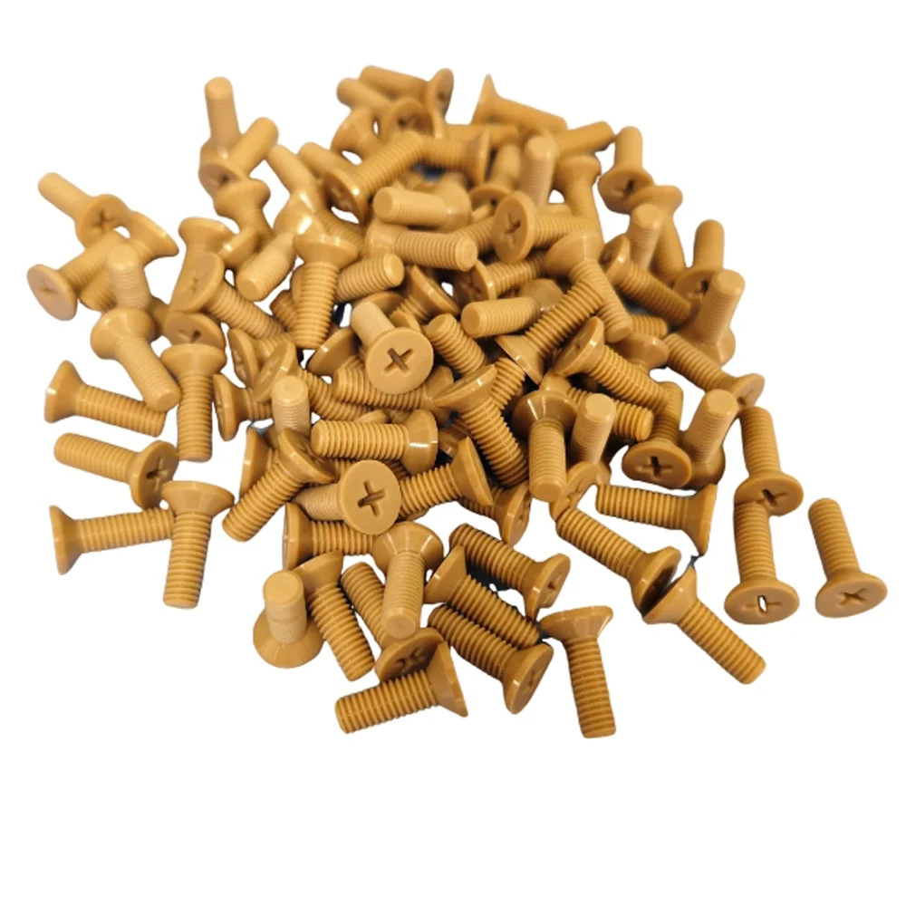 |
Chemical processing equipment: PEEK is used for chemical processing and processing equipment in semiconductor manufacturing plants due to its corrosion resistance to chemicals and ability to maintain structural integrity in harsh chemical environments.
Ion implantation components: Components made of PEEK are used in ion implantation equipment and are exposed to ion beams and reaction gases. The stability of PEEK under radiation and its ability to resist corrosive gases make it highly suitable for these applications.
Measurement and testing equipment: PEEK is used as a component of measurement and testing equipment in semiconductor manufacturing. Its dimensional stability and wear resistance ensure accurate measurement and long-term reliable operation.
Thermal management: The thermal stability and insulation properties of PEEK can be used for thermal management applications in semiconductor devices. It helps to effectively control and dissipate heat in components such as heat exchangers and thermal isolators.
Wafer handling and processing: PEEK components are used in wafer handling robots and tools due to their mechanical strength, wear resistance, and ability to withstand repeated exposure during cleaning processes and wafer transfer operations.
Pump and valve components: PEEK is used for pumps, valves, and fluid handling systems in semiconductor equipment. Its wear resistance, chemical resistance, and ability to maintain strict tolerances ensure the reliable operation of the fluid control system.
Microelectronic packaging: PEEK is used for microelectronic packaging, and its high-performance characteristics help create protective shells and enclosures for sensitive semiconductor devices, providing mechanical protection and electrical insulation.
Service life and maintenance: Components made of PEEK are known for their long service life and reduced maintenance requirements for semiconductor equipment. Its durability and wear resistance can minimize downtime and ensure continuous operation of critical manufacturing processes.
Overall, the unique performance combination of PEEK makes it a multifunctional material in semiconductor equipment, helping to improve the performance, reliability, and lifespan of tools and machinery used in semiconductor manufacturing facilities. Its application scope covers all stages of semiconductor manufacturing, from wafer processing to final packaging, improving the efficiency and effectiveness of the semiconductor production process.